PCB Layout Design
We offer expert PCB layout design services, ensuring optimal performance, efficiency, and reliability for your electronics.
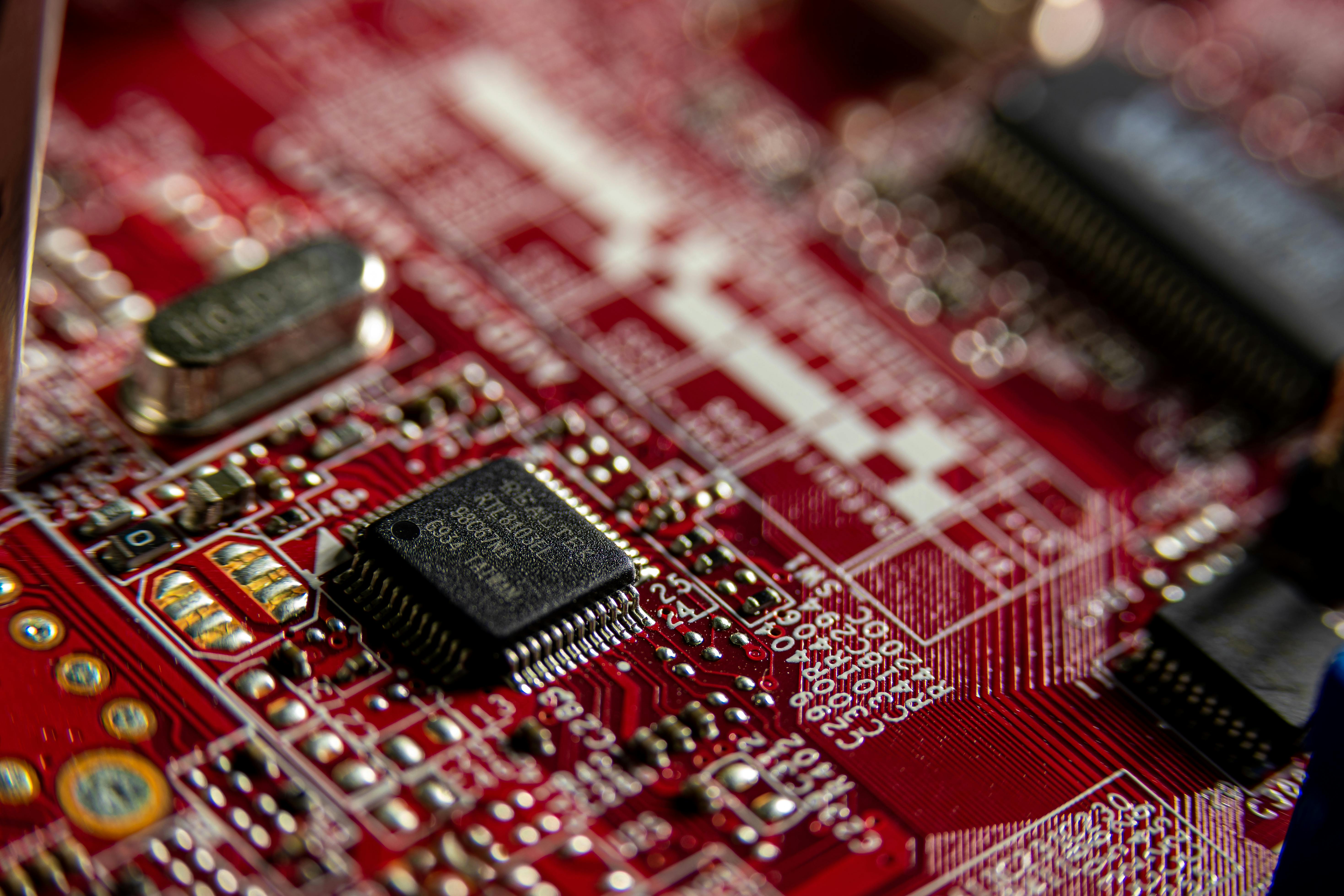
Our team of experienced engineers specializes in designing precise PCB layouts that ensure optimal functionality, electrical performance, and manufacturability. Whether you're working on a simple board or a complex multi-layer design, we ensure that your PCB layout meets the highest standards of quality, efficiency, and performance.
We use state-of-the-art design tools and industry best practices to create layouts that maximize space utilization while minimizing signal interference. Our focus is on providing designs that are easy to manufacture and highly reliable in real-world applications.
Precise and Reliable Layouts
We create precise PCB layouts that minimize errors and ensure optimal performance in your electronics, whether simple or complex designs.
Optimized for Manufacturing
We design layouts that are easy to manufacture, ensuring minimal errors and faster production cycles without compromising quality.
Why Choose Our PCB Layout Design Services?
We provide PCB layout design services that guarantee exceptional performance, precision, and reliability for your electronic products. Our designs ensure efficiency and manufacturability in the most demanding applications.
Custom PCB Layouts
Tailored to your specific needs, our PCB layouts are designed for optimal performance, space utilization, and manufacturability.
High-Density Designs
We specialize in creating high-density PCB layouts that maximize the use of space while maintaining signal integrity and minimizing noise.
Complex Multi-Layer Designs
Our team excels in designing multi-layer PCBs that require precise routing, thermal management, and optimal electrical performance.
Our PCB Layout Design Process
We follow a structured design process to ensure that every PCB layout is optimized for performance, manufacturability, and efficiency. Our approach minimizes design errors and ensures timely delivery.
Design Consultation
We begin by consulting with you to understand your requirements, specifications, and performance goals for your PCB layout design.
Layout Development
Our engineers begin creating the PCB layout, ensuring optimal signal routing, component placement, and power distribution for the design.
Review and Testing
The layout is reviewed and tested for functionality, manufacturability, and compliance with industry standards before final approval.